A recent article in Chip Scale Review “Automotive LiDAR: Photonics assembly requirements and trends” discusses the similarities and differences between automotive light detection and ranging (LiDAR) and optical transceivers. The photonics device assembly requirements and trends in automotive LiDAR are introduced. An assembly solution for automotive LiDAR is explained. Finally, a demonstration of the solution with actual assembly experiments for typical edge-emitting lasers (EELs) and vertical cavity surface emitting lasers (VCSELs) chips for automotive LiDAR are presented.
Photonics devices assembly in automotive LiDAR
“Automotive LiDAR is a complex photonics sensor system that consists of multiple optical components, including lasers, amplifiers, phase and amplitude-control low-noise photodiodes, mode converters, and optical waveguides, etc. Table 1 shows the comparison of automotive LiDAR and optical transceivers. Based on the table entries, automotive LiDAR is in an earlier phase of product life cycle than the optical transceiver.
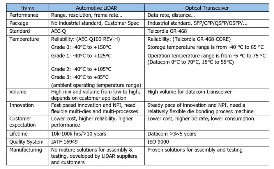
From Table 1, we know automotive LiDAR does not have industry standards for packages and optoelectronics (OE) interfaces at this point in time. The end users of automotive LiDAR have diverse package design requirements to fit it into their cars. This means that the vehicle manufacturers decide on the package form and interface of automotive LiDAR devices. If a LiDAR supplier targets multiple vehicle models from multiple car companies, there will be a wide range of package form factors. Manufacturing in the automotive LiDAR industry, therefore, will be high-mix low-volume for the time being. As a result, LiDAR suppliers have to provide flexible equipment to support different customers’ packaging and assembly process designs.”
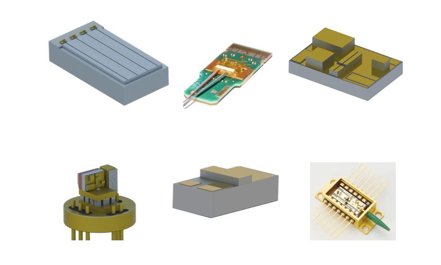
“With the advancement of new technologies, we find that automotive LiDAR imaging technology has evolved from mechanically-scanned LiDAR to hybrid solid-state LiDAR, and then to solid-state LiDAR. The packaging of automotive LiDAR evolved from discrete components to module-level integration, and even chip-level integration (see Figure 1). The market is trending towards highly-integrated, thinner and cheaper products [1-4]. Consequently, higher accuracy assembly is required to manufacture the photonics devices. Automotive LiDAR has a similar photonics device assembly process to that of the optical transceivers, and the assembly accuracy and other requirements are also similar. Depending on the different laser package designs, from 5μm to 0.5μm is the typical high-accuracy requirement for laser die; other parts, however, may have less critical accuracy requirements. In general, most edge-emitting laser dice are attached with a eutectic process (some may use an epoxy process); VCSEL laser dice are usually attached with an epoxy process, and an optical lens with ultraviolet (UV) epoxy plus in situ curing.”
High Precision Die Bonding System Challenges for Optical Components Package Application in Photonics Industry
The Photonics Packaging industry is frequently compared in alignment with the Semiconductor industry thirty years ago. Many existing first generation processes are not necessarily appropriate for photonics packaging manufacturing. Frequent challenges include a high part count, photonics devices placed at various angles and levels, and mixed technologies in a single part, including various eutectic processes (i.e. different reflow temperatures using various metal compositions to achieve a temperature hierarchy), thermally cured epoxy, and epoxy cured by ultra violet light (UV).
High Precision Photonics Packaging
Devices need to be placed in photonics packaging to a high degree of accuracy. The optical path needs to be actively or passively aligned to minimize the scattering of light. While active alignment is frequently done at the final stages of photonics packaging assembly, when aligning the fiber to the photonics packaging, aligning the fiber can be minimized by accurately aligning the individual pieces during assembly. One example of a critical alignment is in aligning an edge-emitting laser to the submount within the photonics packaging system. If the front edge of the chip overhangs the submount the device does not receive a good surface to dissipate heat, resulting in overheating and failure. And yet, if it does not reach the edge of the submount then the light signal is reflected off the submount and the signal is reduced.
Solution for Achieving High Accuracy
Placement accuracy is of paramount importance in photonics packaging assembly. Laser die demand accuracy for heat dissipation and to minimize reflection. Photodetectors must be placed in line with the beam. Passive elements frequently offer very small areas which must be aligned in order for a beam to pass.
To achieve this level of accuracy for photonics packaging, automated assembly equipment must start with the right platform. The platform must be composed of materials that are stable regardless of temperature or humidity fluctuations. This can be achieved with granite or advanced polymers. For motion control, linear motors with optical encoders can be used for rapid and accurate movements with very high precision. To maintain the accuracies of the robot at the work surface, it is important to minimize the separation between the robot axes and the actual work surface. Cantilevered robots can suffer serious losses in accuracy and speed. Integration of machine vision combines the accuracy of the machine with the ability to deal with variably presented parts. For automated photonics packaging assembly to be effective, the system design must ensure that frequent calibration is not necessary.
Photonics Packaging Automation Solutions
While the automation technology of manufacturing of photonics packaging presents some unique requirements and challenges, it is possible to achieve success coupling reduced costs and increased capacity. Automation can be extended to dispensing, assembly and integration to further reduce costs and increase capacity down the line. Further automation can be applied to handling systems for submounts to augment throughput and reduce operator handling.
Eutectic Bonding
Another key factor in the successful scaling of photonics packaging manufacturing, is the use of eutectic bonding. Eutectic bonding is the process of using a solder alloy as a third material to form a continuous bond between two components. In the case of photonics packaging, this often means two gold-plated materials coupling by lead-tin, gold-tin or gold-germanium solder. To achieve this bond, typically, a solder preform is placed on one component, usually a carrier or submount. Then, the second component, often a MMIC, photodetector or laser chip, is placed on the preform. The temperature of the assembly is brought up to just above the melting point of the solder either by heating the base on which the assembly rests, or by flowing heated gas over the assembly. Just as the solder liquefies, the chip is placed with a controlled force. The part is cooled to below the reflow temperature enabling the eutectic bond to be complete. Depending upon the device type and construction, scrubbing may be used during the placement process. It is therefore a crucial assembly technology for successful manufacturing of a photonics packaging system.
Optical Network Components (Driving Photonics Packaging)
Read the latest MRSI Blog: Challenges and Solutions in the #Photonics Packaging Industry https://t.co/TykdRt04tr pic.twitter.com/09vDZRDdlh
— MRSI Systems (@mrsi_systems) October 18, 2017
As mentioned earlier, the significance of optical networks is demonstrated by the vast array of commonly used components within telecommunications and data communications including the following:
- Optical Transmitters
- Optical Receivers
- Optical Fibers
- Switches
- Amplifiers
- Photo detectors
- MUX & DEMUX sub-components
- Tunable devices
The ubiquitous nature of these photonic components and their related vast array of factors continues to ensure dramatic increases in demand for the manufacturing of Photonics Packaging.
MRSI Systems Photonics Packaging
MRSI Systems has been serving the photonics packaging technology customers for over 40 years and understands their requirement to scale efficiently in today’s fast paced microelectronics and optoelectronics marketplaces. Automating the assembly of photonics packaging is readily achieved with MRSI Systems’ die bonders and epoxy dispensing solutions. Automation is essential for photonics packaging to achieve high throughput and yield that this growing market demands. Our advanced systems enable companies to scale from prototype to high volume manufacturing of optical devices efficiently.
Contact MRSI Systems to learn more about our Photonics Packaging solutions.
About MRSI Systems
MRSI Systems (a part of Mycronic Group) is the leading manufacturer of fully automated, high-speed, high-precision and flexible eutectic and epoxy die bonding systems. We offer solutions for research and development, low-to-medium volume production, and high-volume manufacturing of photonic devices such as lasers, detectors, modulators, AOCs, WDM/EML TO-Cans, Optical transceivers, LiDAR, VR/AR, sensors, silicon photonics, co-packaging optics, 3-D hybrid packaging, and optical imaging products. With 40+ years of industry experience and our worldwide local technical support team, we provide the most effective systems and assembly solutions for all packaging levels including chip-on-wafer (CoW), chip-on-carrier (CoC), PCB, and gold-box packaging. For more information visit www.mrsisystems.com
About Mycronic
Mycronic is a Swedish high-tech company engaged in the development, manufacture and marketing of production equipment with high precision and flexibility requirements for the electronics industry. Mycronic’s headquarters are located in Täby, north of Stockholm and the Group has subsidiaries in China, France, Germany, Japan, Mexico, the Netherlands, Singapore, South Korea, United Kingdom, the United States and Vietnam. Mycronic is listed on Nasdaq Stockholm. www.mycronic.com