In this post we examine the critical manufacturing challenges facing Photonic Device manufacturers as they scale up to meet unprecedented demand. Specifically, we explain the issues surrounding CoS and how die bonders have evolved to meet the new demands of the industry.
Within the Datacom market, the photonics packaging segment is experiencing increasing demand for data and bandwidth leading to the demand for high-volume manufacturing (HVM) of photonics devices. This expansion is driven by the increased demand for Internet of Things (IoT) applications, data consumption from cloud computing, web and mobile based applications, and storage through hyperscale data centers.
CoS Explained
Among the critical building blocks for the successful high-volume manufacturing of photonic device, are the CoS devices to deliver the required performance, reliability and volume. CoS devices present some unique manufacturing challenges. As a result, application-specific die bonders have evolved over decades to address the current manufacturing demands of CoS. We will now examine the two basic elements of CoS, the laser diode (LD) CoS and the photodetector (PD) CoS in more detail.
In fiber optic transmission the laser diode (LD) CoS, also referred to as a chip-on-carrier (CoC), is the starting point of light generation and transmission, and the photodetector (PD) CoS is the ending point of the light, which is received and translated into an electronic signal. It is quite typical for a 100Gbps fiber transmission to have four sets of LD and PD CoS at a rate of 25Gbps each. Some have 10 sets at a rate of 10Gbps each. The quantity of LD CoS and PD CoS can therefore be four to ten times the quantity of final optical modules.
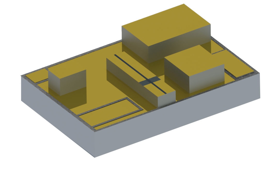
A common configuration of a LD CoS, includes a eutectically bonded LD and a back facet monitoring detector, both mounted on the same submount. The quality of the joint between the LD or PD chip to the submount is one of the most critical factors for device long-term reliability. Eutectic bonding is used for a highly thermally efficient interconnect with long-term reliability. The LD CoS may include additional components, such as thermistors, capacitors and driver chips. The PD CoS typically includes a PD and may also include additional components, such as a transimpedence amplifier (TIA), and in some cases, a thermistor for temperature control. In subsequent process steps the completed CoS may be mounted onto a thermoelectric cooler (TEC) packaged in a “gold box” or TO-Can package. We will now discuss how eutectic bonding can be optimized for CoS.
Eutectic Bonding Optimized for CoS
In order to achieve the eutectic bonding of these multiple parts within the package, a temperature hierarchy of eutectic solder is frequently required. When using a TO-Can package, it is common that the LD and the monitoring detector are each eutectically bonded on separate CoS and then mounted in a vertical plane just offset from 90 degrees of each other.
Because of high power requirements, small component sizes, and the need for the elimination of materials that outgas, many components are attached with a eutectic die bonding process. The CoS substrate sizes are small, typically less than a few millimeters. A small form factor eutectic stage is needed to provide ultra-fast temperature ramping, and ultra-fast cooling cycles. A closed-loop, low-mass, high-power, pulsed heated eutectic stage is required. Stable temperature control and cover gas flow must be optimized throughout the eutectic process. Additionally, the eutectic station must be fully programmable, tailoring the process for a specific bonding recipe. Faster speeds, higher yields and repeatable quality are the outcomes.
Eutectic bonding is the process of using a solder alloy as a third material to form a continuous bond between two components. In the case of CoS, this often means two gold-plated materials being joined by gold-tin solder. When performing eutectic die bonding, the temperature of the assembly is brought up to just above the melting point of the solder. As the solder liquifies, the chip is placed with controlled force. The part is then cooled to below the reflow temperature and the eutectic bond is complete. During the time that the part is subjected to heat, it is important to control the atmosphere. Eutectic bonding is usually performed in an inert environment to prevent oxidation of the bonding surfaces. A 95-5% nitrogen-hydrogen mix should be used so that hydrogen is present for use in the formation of the bond.
Overall high-volume manufacturing of photonics packaging is challenging, which must be solved by optimizing processes, such as eutectic bonding of CoS. These high-volume manufacturing solutions are essential to increase product and produce repeatable quality.
Learn more about our die bonding solutions and Eutectic Bonding.