DIE BONDING
Die bonding is a manufacturing process used in the packaging of semiconductors. It is the act of attaching a die (or chip) to a substrate or package by epoxy or solder, also known as die placement or die attach. The process starts with picking a die from a wafer or waffle pack and then placing it at a specific location on the substrate. The die is placed into a previously dispensed epoxy or placed into solder (eutectic). Historically, the levels of electronics assembly were:
- Level 1 – Die Assembly
Interconnection of the bare IC to its underlying circuitized substrate. The substrate material, mostly ceramic and metal leadframes, were originally selected based on thermal (coefficient of thermal expansion) and reliability requirements. Typically, die bonding was done on the top side, with interconnection points to the next level on the bottom side (typically pins in through holes). The interconnect layer is the die bonding material. Cavity and bottom side bonding was subsequently introduced, along with the addition of non-active components, passives and discretes. The end-product of this assembly step was (and still is) the IC package.
- Level 2 – Printed Circuit Board assembly
Multiple IC packages, as well as necessary capacitors, resistors and discrete components were bonded or inserted to or into a printed circuit board (PCB). PCB boards would typically consist of power and signal layers of etched copper in a fiberglass reinforced matric (FR4 for example). Connection to the next level was made through end-connectors. Today, some direct die-to-board bonding is performed, in a convergence of level 1 and 2. In fact, in some advanced assembly, some die are mounted in inner layers of the board (embedded components).
- Level 3 – Panel Assembly
Multiple PCB Boards were inserted into a final panel, ready to connect to the outside world through the usual electrical connection points.
- Level 4 – Final Assembly
As the name implies, this step consists of packaging the end-product. Typical steps would be to place the electronics in a final case, connecting power cables, etc. In many cases today, these steps are fully automated.

Die on Submount
As with all technology development over history, the mantra of“smaller, faster, cheaper” has fueled constant innovations in the drive to collapse all of these packaging levels. Today, we can easily find products with three (3) levels of assembly. In essence, circuit density has enabled the elimination of multiboard systems, essentially eliminating Level 3 Panel Assembly. Mobile phones are a good example of a 3-level product (microcontroller module assembly, main mobile motherboard assembly, and final packaging). To find two-level products, small standalone sensors come to mind, perhaps communicating a simple function wirelessly, using a phone app.
Whatever level of convergence we encounter in today’s novel products, die bonding remains an ever-present step in the manufacturing of electronics. It lies at the necessary juncture of semiconductor manufacturing and semiconductor assembly. Dice can be bonded to a base substrate (Level 1), or it can be bonded to a printed circuit board alongside other components and ICs (chip-on-board) (Level 2).
Die Bonding can thereby be succinctly described as the placement of a semiconductor device onto the next level of interconnection, whether it be a substrate or a board. It is referred to in the industry as die placement, die attach, or die bonding. Although the objective is the same, die bonding processes and die bonding equipment vary greatly, depending on functionality, cost, performance, size, hermeticity, product life expectancy, and required reliability.

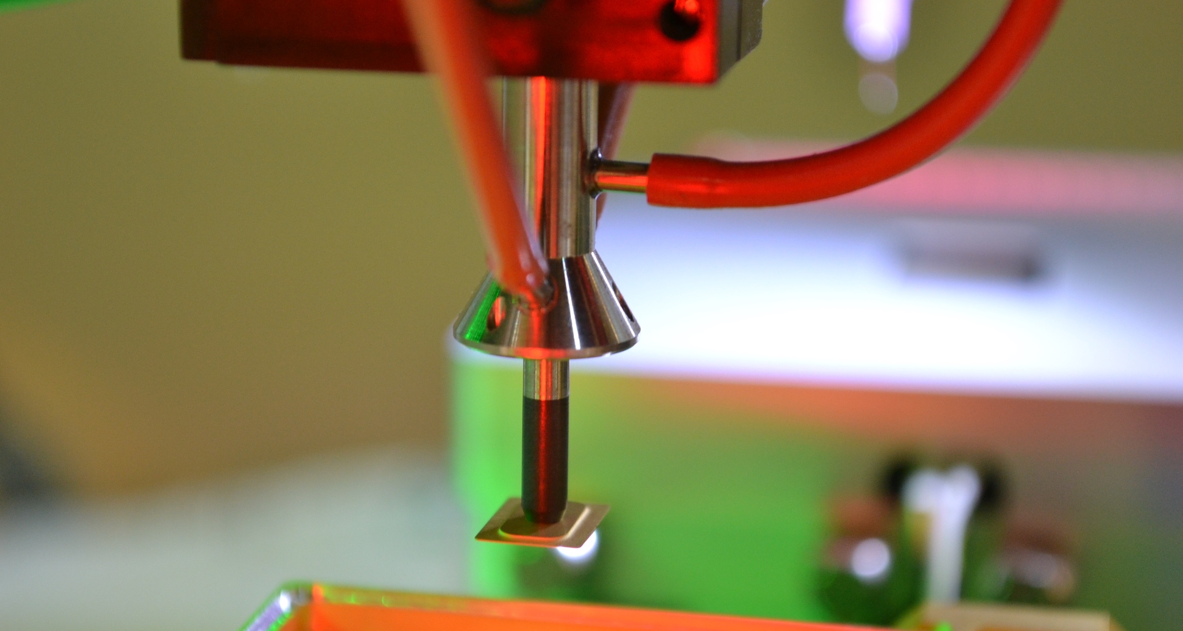
Image of Real Time Video Pick & Place Tip
Various die bonding approaches have been, and still are, developed to meet the ever-evolving product requirements. Such approaches include:
- Epoxy Die Bonding combined with either batch, continuous or in-situ curing
- Eutectic Die Bonding and in-situ reflow
- Flip Chip Attachment combined with either standalone or in-situ curing
Die bonding process selection is based on the application. Balancing cost, performance and reliability is usually involved. Reliability Classes are well defined (consumer, computer and data communications, military/aerospace, telecommunications, and harsh environments). They mainly differ in their thermal cycling and hermiticity requirements. Thermal cycling is a common metric. Parts are placed inside a humidity chamber and must typically meet a certain number of thermal cycles without failure. Most failures occur at the material interfaces due to thermal expansion mismatches. Therefore, the integrity and performance of the die attach layer is often seen as critical. This means that the choice of the die attach material, its curing profile, and the thickness of the bond layer are all critical parameters in the quest to meet such reliability requirements. The size of the die, the thickness of the die, the coefficients of thermal expansion of the die, the substrate and the die attach material are all factors to be considered.
The operating environment also drives the choice of the die bonding process. Consumer products used inside the home or the office would have a different requirement than an optoelectronics module operating outside, or in the sea bed, that needs to operate reliably between -40F to +40F in a harsh environment. Satellite, military, and aerospace parts would have also a different requirement. The die bonding process will be different for a product that needs to be completely hermetic versus a consumer product that has an expected 3-year life in an office. In a hermetic package, concerns of degassing and humidity, build-up would tend to support non-polymer based constructions (eutectic die bonding versus epoxy die bonding).
Finally, products have different performance requirements. An IC used in microwave radar applications, has a completely different material set, and general product requirements than the electronics found in a TV remote controller.

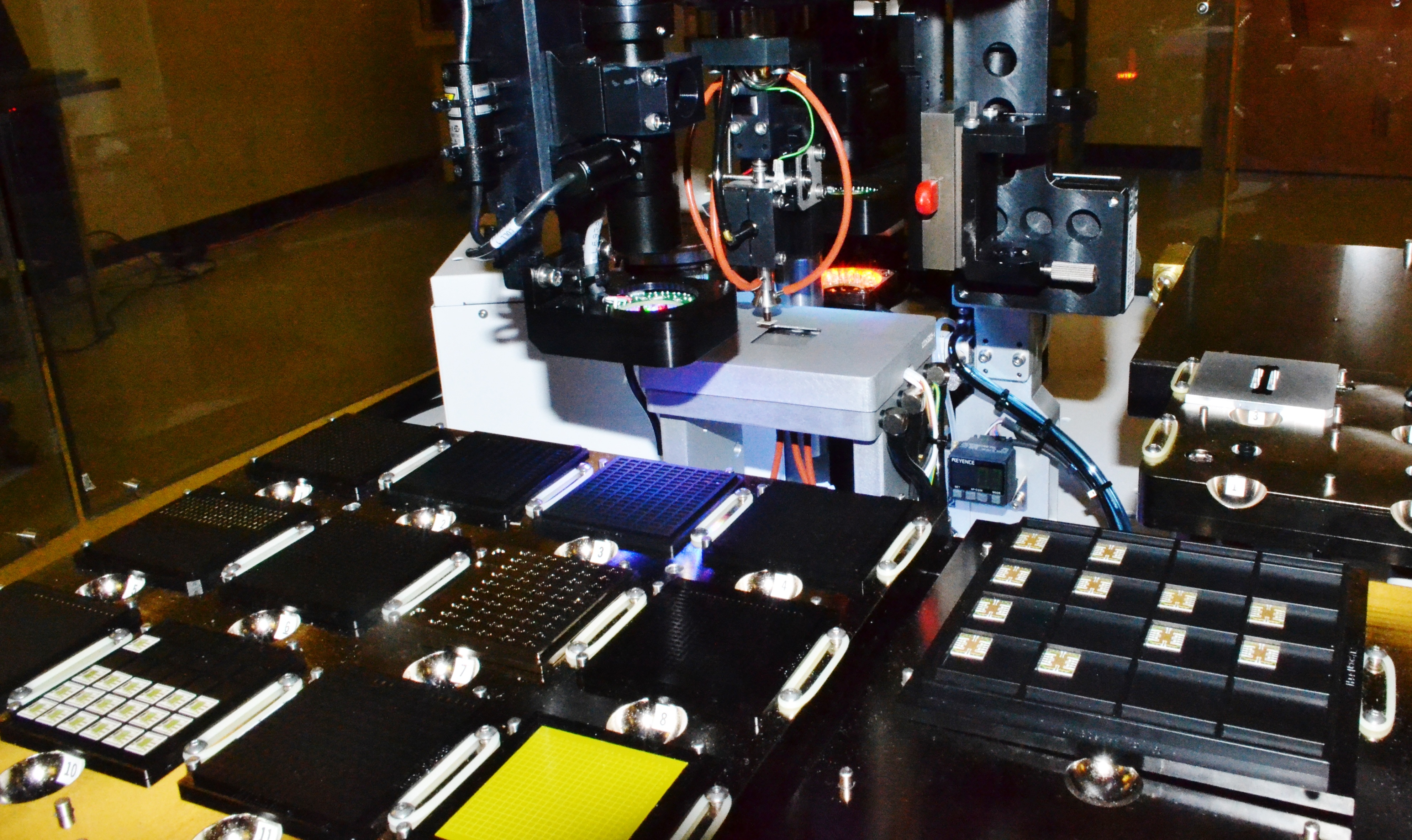
MRSI-705 Die Bonding
Performance, reliability and environmental requirements must be met at the lowest cost possible. Levels of automation, process speed, and optimized throughput are all factors that a packaging engineer will consider to balance requirements with manufacturing costs.
Similar to the die bonding process, the die bonding equipment varies greatly based on the end product specification requirements. Die bonding equipment for the assembly of high volume consumer products, with its lower reliability and environmental requirements, will consequently be quite different than die bonding equipment dedicated to high reliability telecommunications packages. In the latter case, higher accuracy is required, process repeatability and process control are paramount, and the overall reliability of the interconnect is critical.
Finally, the case of Datacom applications is quite unique. Although the environment requirements are not as stringent as Telecom; the performance of the package, and in particular as it pertains to the speed of data transactions, drive a unique need for ultrafast off-chip, and even on-chip performance. This is where photonics assembly comes into play. Die bonding approaches for this application are novel, needing high accuracy placement for passive alignment, while leveraging the speed of known epoxy die bonding techniques. MRSI is well positioned for such applications, refer to Optoelectronics Die Bonding for more information on this front.
Learn more about MRSI Systems’ Die Bonding and Epoxy Dispensing Solutions.
