Key Elements in Achieving Accurate Local and Global Alignments
Having a proven ultra-accurate die bonding system platform that is mechanically and thermally stable, with no cantilevered parts, are essential elements to achieve accurate device placement. In addition, the accurate alignment of device fiducials is required to achieve micron-level accuracies. Achieving alignment to ensure accurate final placement of parts in die bonding, requires highly specialized software and proven alignment techniques.
Die Bonding Alignment Software
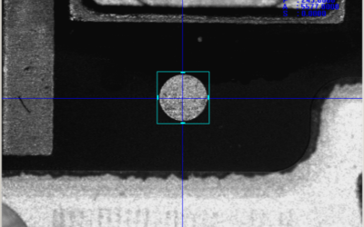
Local and global vision alignment is used for nested substrates and feature alignment. The die bonding software must allow the user to align die relative to substrate fiducials, die edges, or features of previously placed dice. Precise placement of the die in a microwave circuit allows the designer to control attenuation of the circuit and greatly reduce or eliminate tuning after assembly, which can significantly reduce assembly costs. The alignment of the laser chip to photo diode or a lens to a VCSEL are common photonic examples. A unique software feature of the MRSI die bonding systems is the Split Fiducial. This feature allows the use of separate fiducials for the X and Y axis. In optical applications this permits the laser stripe to be used in one axis and the die face in the other axis. Another example is the alignment of critical die such as MMICs and beam lead diodes. This capability ensures repeatability and precise alignment of optical and microwave devices.
Alignment Techniques for Die Bonding
Proper, correct and precise alignment of the die is possibly the most important process parameter in the manufacturing process. Regardless of the package style, alignment is always critical and it is important to employ the correct alignment scheme for placement of the chip and subsequent attachment. There are two different alignment schemes that can be used:
- Active or “Real Time” Alignment
- Passive “Dead Reckoning” Alignment
A particular package style will favor one of the above listed alignment schemes. And for a successful and “robust” alignment process, the best fit alignment scheme for that package must be used. That alignment scheme must then be supported by the proper selection of optics and lighting.
Active or “Real Time” Alignment in Die Bonding
The die is viewed in a position above the spot on the package where it needs to be placed, either through a clear substrate or through a window in a substrate. After final alignment, it is placed down in real time. The viewing camera is located directly beneath the substrate and is actually viewed through the substrate. Therefore, placement is guided and is inherently more accurate.
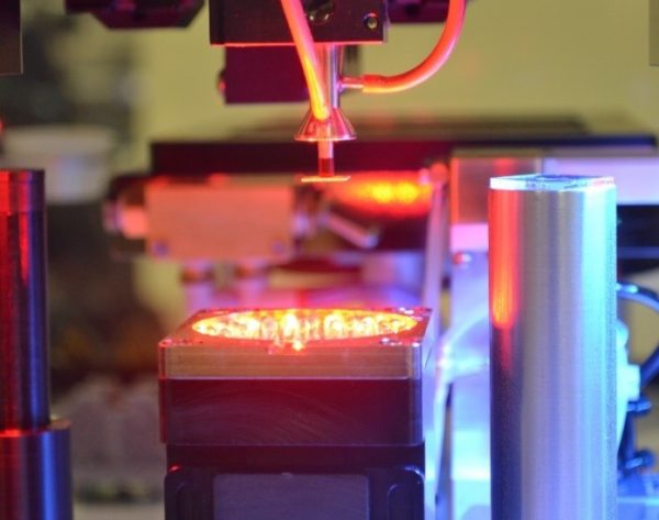
In die bonding applications where there is a transparent substrate such as a row or column driver on a flat panel display, the chip can be placed in the near alignment position above the pad traces. The camera then locates the chip in real time. The up/down viewing optical probe the moves into position between the substrate and the device. Final alignment is the made using machine vision aligning to the die and substrate fiducials in real time. The optical probe then retracts and the device is placed onto the substrate.
The basic concept of active alignment in die bonding is to bring the component close to the target so the component and the target can be processed in the same image for further X-Y and theta corrections.
The major benefit of this methodology is that final placement accuracy can be anticipated before placing the component.
Die Bonding – Passive “Dead Reckoning” Alignment
Nautically speaking, navigation by dead reckoning or originally “deduced reckoning,” is the process of figuring out your current location by calculating known course, speed, last confirmed location and other factors. Dead reckoning alignment is not much different.
In dead reckoning alignment, alignment measurement is carefully done in one specific area of the die bonding system, and then the die is moved to another part of the die bonding system and placed. It is not necessarily a move of any great distance, but it is a calculated move. After the move, no further alignment check is done prior to placement. Relying on a calculated move also requires faith in the die bonding system and its precision; because, there is no way to verify whether placement is correct after a horizontal relocation from the alignment site.
Passive alignment normally involves a set of pre-calibration procedures that establishes geometrical relationships among die bonding system devices, including the vision system, the pick-and-place head and theta center. All subsequent operations use these calibration results, which is the reason why this methodology is also called the pre-calibrated alignment technique.
In passive alignment of a flip chip like device, an upward-facing camera is used to locate and orient the features on the bottom side of a chip. A downward facing camera aligns the features on the substrate. A highly accurate X-Y motion system then places the chip onto the substrate, based on a calculated offset. This type of alignment is used for most flip chip processes.
If you have die bonding challenges, contact our Customer Support Team.
About MRSI Systems – Die Bonding and Epoxy Dispenser Solutions
MRSI Systems is a leading manufacturer of fully automated, high-precision, high-speed die bonding and epoxy dispensing systems. We enable customers to optimize the performance of their process including yield, throughput, and uptime by building systems that use our unique expertise. In summary, this includes our proprietary software, proven hardware, deep process knowledge, state-of-the-art manufacturing, and a world-class customer service team. MRSI’s systems are built on common platforms that can be configured to meet specific customer requirements. These platforms are designed to be scalable for R&D prototyping, pilot production and high volume manufacturing. Our solutions deliver the best financial returns in the industry while integrating seamlessly into our customer’s production. Markets include Telecom/Datacom (Data Center), Aerospace & Defense, Medical Devices, Computers and Peripherals, and Industrial. Since 1984, we have been recognized as the standard of the industry, delivering our solutions to leading optoelectronic and microelectronic customers worldwide. We are headquartered in Billerica, MA in the greater Boston area. Our sales are supported by a global network of direct service and support professionals, located in China, Taiwan, Singapore, Korea, Thailand, Malaysia, the Philippines, Israel, Europe, United Kingdom, and the United States.


