WAFER LEVEL PACKAGING
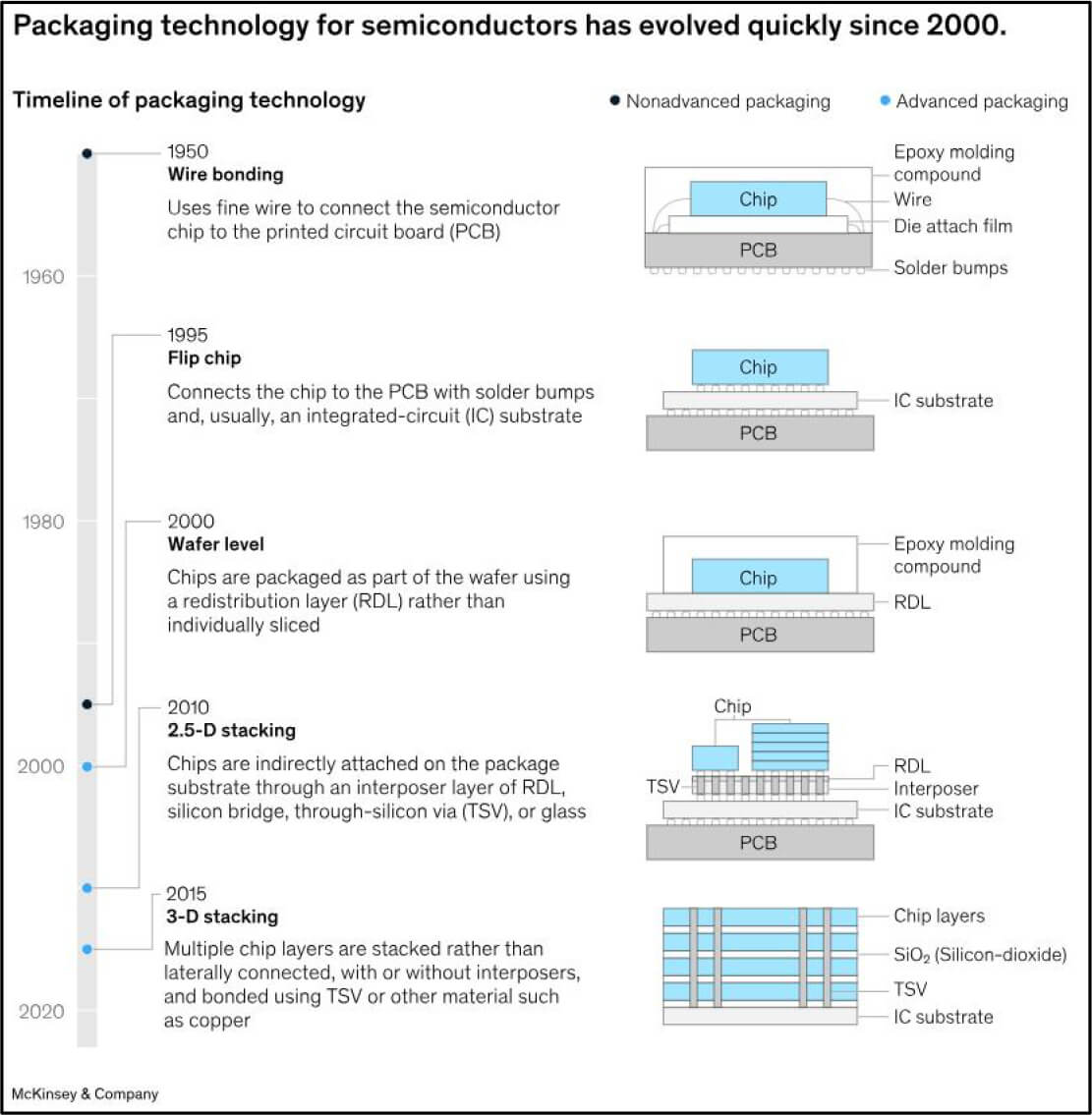
As the semiconductor industry propels into an era of unprecedented advancement and growth, advanced packaging solutions through wafer-level packaging stands to support record breaking demand. Wafer-level packaging (WLP) has been growing continuously in electronics packaging due to its low cost in batch manufacturing. Wafer-level packaging is a process where electronic components such as a chip, memory, BGA, and other die are attached to the wafer directly.

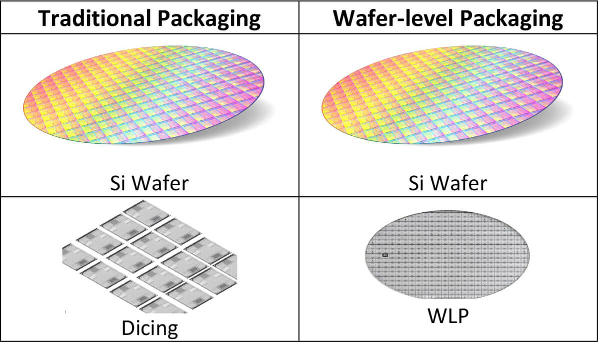
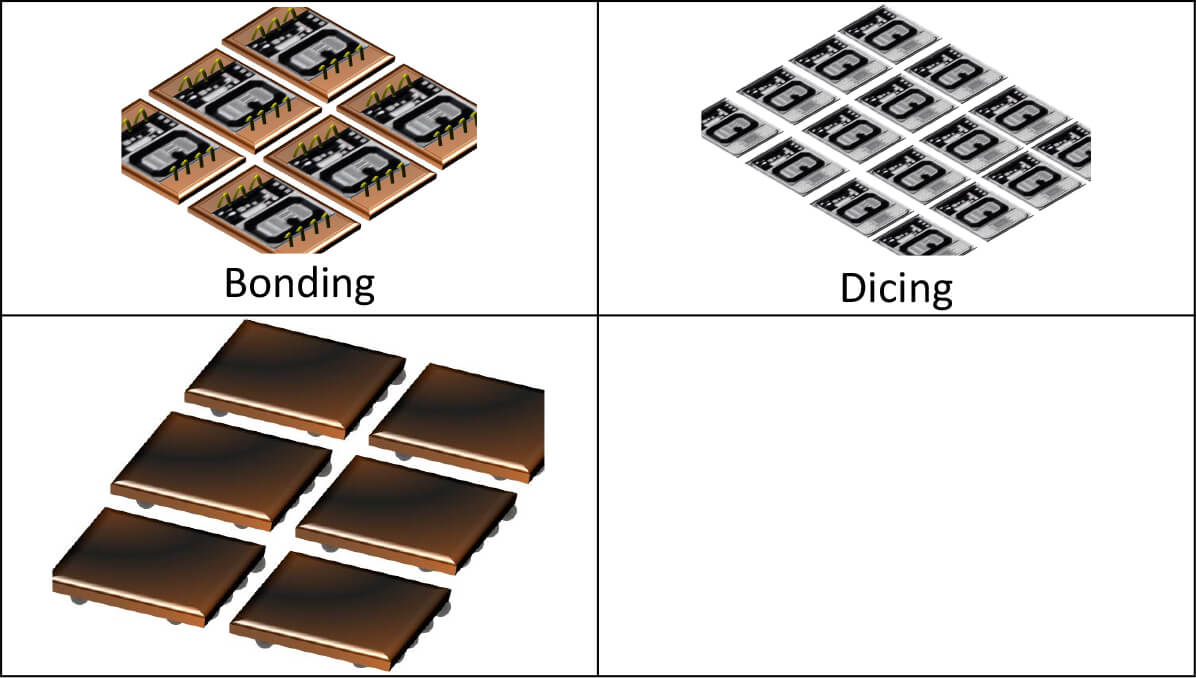
Traditional vs WLP:


Fan-In WLP and Fan-Out WLP:
Fan-in wafer-level packaging refers to packaging an IC chip directly on the wafer, unlike the traditional method of placing each IC chip on a diced wafer. FI-WLP is an extension of WLP that uses the traditional process with the exception of bumps instead of wire bonding that provides the interconnection to the chip with the wafer. Fan-out wafer-level packaging is an advanced WLP, enabling a higher number of semiconductor passive components, dies, and sometimes MEMS integration and packaging onto a single wafer substrate.
FOWLP is gaining acceptance in the industry because it is a near alternative to TSVs (Through Silicon Vias) and a cost-effective way of achieving higher interconnect densities in compact spaces. This allows packages to become thinner and have a greater range of form factors.
End Markets and Applications:
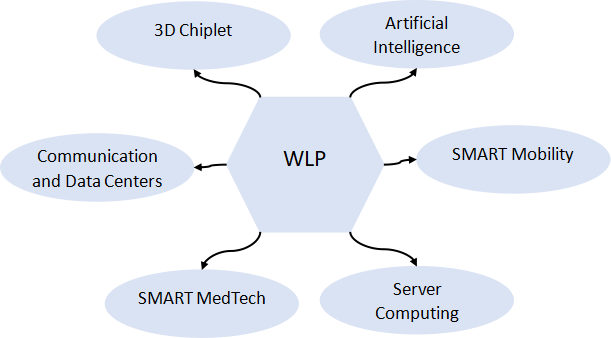
The versatility of wafer-level packaging makes it a go-to solution for numerous applications across industries, offering benefits such as miniaturization, improved electrical performance, cost efficiency, and reliability. The emerging development in Artificial Intelligence (AI), E-Mobility, Internet of Things (IoT), and Aerospace and Defense markets have opened endless WLP applications.

The introduction of 2.5D and 3D advanced chip packaging has changed the competitive landscape for semiconductor chip manufacturing. Certainly, further advanced packaging in the WLP market offers disruptive opportunities in almost all markets and segments.
In conclusion,
MRSI system’s H-LD, HVM and S-HVM systems are equipped with the advanced functions and features required for the Wafer Level Packaging.
MRSI Systems
MRSI Systems (a part of Mycronic Group) is the leading manufacturer of fully automated, high-speed, high-precision and flexible eutectic and epoxy die bonding systems. We offer solutions for research and development, low-to-medium volume production, and high-volume manufacturing of photonic devices such as lasers, detectors, modulators, AOCs, WDM/EML TO-Cans, Optical transceivers, LiDAR, VR/AR, sensors, silicon photonics, co-packaging optics, 3-D hybrid packaging, and optical imaging products. With 40 years of industry experience and our worldwide local technical support team, we provide the most effective systems and assembly solutions for all packaging levels including chip-on-wafer (CoW), chip-on-carrier (CoC), PCB, and gold-box packaging. For more information visit www.mrsisystems.com
