SILICON PHOTONICS
The Silicon Photonics market is set to grow in size from around $480m as measured in 2019 to around $3.9B by 2025 according to the global analyst firm Yole. We describe below the drivers behind this growth and how MRSI is supporting our manufacturing customers to capitalize on this new technology.
What is silicon photonics?
Silicon photonics is the application of silicon as an optical medium in the design and manufacturing of photonic devices. These devices are used for a variety of applications, including high-speed data communication, LIDAR for autonomous driving, advanced optical sensors in consumer electronics and life science, and high performance computing. Silicon is typically patterned with sub-micron resolution into photonic components using well-established semiconductor fabrication processes and proven equipment, often in the same fab in which ICs are fabricated. The use of silicon as a platform for photonics allows for the integration of optical and electrical components on a single chip, enabling the creation of compact low power consumption and cost-effective systems.
It is a promising technology that offers significant benefits in scaling up data capacity. It is expected to play a crucial role in the development of next-generation communication and computing systems as well as many other emerging fields, many companies have developed platforms for automating the process of designing and fabricating silicon photonics components. These platforms will drive the adoption of this technology in a range of industries.
What are the advantages of silicon photonics?
One of the main advantages is the ability to process large amounts of data at high speed within a compact footprint, making it an attractive solution for users who require high-bandwidth and high data density communication. Some more significant advantages are:
Cost
First, the low production cost for chips. These devices are fabricated using the same CMOS (Complementary Metal Oxide Semiconductor) process on silicon wafers that are widely used by the semiconductor industry. The ability to leverage this established process and infrastructure enables the manufacturing to be low-cost and high-volume, potentially allowing optical devices to be as cheap as their electronics counterpart.
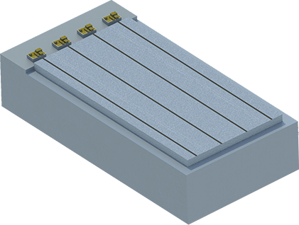
Second, in addition, the use of silicon, which has a high refractive index and low absorption material for light in the communication bands, allows the integration of many devices to be fabricated on one silicon wafer of up to 300mm in diameter. This means a once complex optical module, painstakingly packaged using manual active alignment processes and consisting of photodetectors, modulators, splitter and combiners, AWGs, and more, can now be fabricated onto a single chip approximately 40mm wide. This greatly saves on packaging costs.
Bandwidth
Silicon photonics is the enabler of future bandwidth growth. The savings achieved from device integration in it are not limited to die fabrication and packaging alone. As the telecom and datacom industries evolve beyond 400G into 800G and even higher wavelengths, high bandwidth density and low power consumption are not just amenities but increasingly necessities for the carriers and data center operators, who are running out of floor space and electrical power. Here, the space and power savings inherently offered by silicon photonics enables the industry to pack a lot more bandwidth in a given volume and power consumption budget. It is what the industry needs to keep growing on its current trajectory for the foreseeable future.
Benefits of Scaling
Silicon photonics is a promising industry. It is one of the fastest-growing photonics sectors. In addition to the evidence cited from Yole above, according to ResearchAndMarkets.com, it is expected to grow from $800M in 2019 to $3.7B by 2027, with a CAGR of 21.4%. Leaders across the Communication and IT industries recognize the importance of this technology. All key players including, component makers, many system OEMs, and a large number of university labs continue to invest heavily in its development. And the function doesn’t stop at communication and IT. Many other industries can take advantage of the modular design library of micro-photonic devices and create non-communication devices. LiDAR and advanced sensing are among the first to take advantage of these technologies. As the technologies gain traction driving costs down further, it is expected that more and more applications will emerge from across the globe.
Why MRSI?
MRSI is in a strong position to support the explosive growth of silicon photonics players.
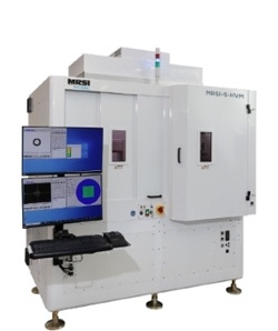
MRSI, being the world’s leader in high precision, high volume, and high flexibility die bonding equipment, is well positioned to serve the silicon photonics demand in the industry. Building on a long line of increasingly accurate die bonders, MRSI recently introduced its sub-micron product MRSI-S-HVM. High-precision bonding of dies on silicon photonics wafers is critical for realizing the full potential of this technology, and MRSI-S-HVM is tailored to do exactly that.
Precision
Despite its many advantages, silicon is not a good material for making semiconductor lasers. Because of its crystalline structure, silicon is an indirect band gap material, making it difficult for electrons and holes to undergo radiative recombination in a silicon diode. That’s why so far, all commercially available laser diodes are still and will continue to be made for the foreseeable future with III-V materials such as indium phosphide and gallium arsenide. However, scientists continue to research innovative ways to make all-silicon lasers a reality with variable degrees of success. Since these devices are often needed in an optical module, the solution is to bond III-V laser dies directly onto a silicon photonics wafer using wafer-level packaging. The bonding process must be highly accurate, typically with a 3-sigma accuracy of below 1 µm, to provide either passive alignment between the laser diode and the silicon photonics chip or make active alignment faster and with higher coupling efficiency. The MRSI-S-HVM die bonder is designed to flip-bond die picked from an III-V wafer onto a silicon wafer (up to 12 inches) using a void-free eutectic process for high-volume manufacturing. An advanced alignment system provides 0.5 µm placement accuracy. To accommodate a diverse range of die and wafer designs, three heating options are available, high-density top heating, bottom thermal heating, and MRSI’s proprietary bottom laser soldering solution.
Flexibility
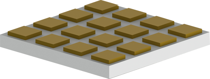
While in theory electric ICs such as laser drivers, TIAs and limiting amps, CDR and many others can be integrated with silicon photonic optical micro-devices on the same wafer, in practice this is not done. Electric ICs have much smaller feature sizes and are often fabricated using the highest-resolution machines available. Optical devices are much larger, their feature sizes comparable to the wavelength of light passing through. Therefore, it’s both difficult and uneconomical to fabricate both electric and optical devices using the same set of equipment. A more realistic approach is to bond ICs with integrated functions onto silicon photonics wafers with, again, wafer-level packaging. Oftentimes, several ICs are bonded to silicon photonics wafers, hence requiring the die-bonding equipment to be flexible enough to handle multiple dies at the same time. The MRSI-S-HVM die bonder is designed to bond multiple dies using multiple processes on the same wafer without the need to switch machines or swap tooling. It brings unparalleled flexibility to the manufacturing. Tools suitable for handling anything from a 150 µm laser die to a 15 mm square sensor array can be changed automatically during processing, and eutectic, DAF, epoxy dispensing, and stamping processes can be implemented at the touch of a keystroke.
In summary, MRSI’s deep expertise in designing high-precision equipment for manufacturing, embodied in the newest MRSI-S-HVM sub-micron die bonder, enables the next level of integration in silicon photonics. With our MRSI solution, customers can achieve low cost, high volume, and high flexibility manufacturing, and meet challenges presented by today’s fast-changing photonics technology business.
Contact MRSI Systems – Advanced Products for Silicon Photonics Packaging Technology
MRSI Systems has been an industry leader offering a portfolio of products ranging from research and development to high-volume manufacturing. Our company, MRSI has a world-class customer support team that has over 35 years of product and technology experience. Contact MRSI to learn more about the products our company has to offer.

QUICK CONTACT
Have Questions about this or other MRSI Systems products?
[caldera_form id=”CF597651fd151d8″]
CONTACT US
Die Attach
-
Eutectic
-
Epoxy stamping
-
0.5μm, 1.5μm
-
Chip-on-Carrier (CoC), Chip-on-Submount (CoS)
Lens Attach
-
UV epoxy dispensing
-
In-situ UV curing
-
Placement accuracy options: 0.5μm, 1.5μm
-
Passive Optical Alignment
Gold-box Packaging
-
Thermal and UV Epoxy
-
Eutectic
-
Placement accuracy options: 0.5μm, 1.5μm