MRSI-705 Equipped with New High Precision Tape Feeders for Very Small Parts
Challenge
As consumers expect more power and more bandwidth from their devices, we see the Advanced Electronic Packaging industry under continuing pressure to cram more technology into smaller spaces. One of the key components to achieve this are called ceramic capacitors. A ceramic capacitor is a fixed-value capacitor in which ceramic material acts as the dielectric. It is constructed of two or more alternating layers of ceramic and a metal layer acting as the electrodes. The composition of the ceramic material defines the electrical behavior and therefore applications. Electronic device manufacturers continue to reduce the size of these ceramic capacitors to become ultra small ceramic capacitors to meet customer requirements. The challenge for manufacturers is finding an epoxy die bonding system that accurately deposits ultra-small amounts of epoxy precisely. Die bonding entails locating and handling these extremely small parts. Common ultra-small capacitor case sizes include 01005 (1.0 x 0.5mm, 0.016″ x 0.008″) and 0201 size (0.25 mm x 0.125 mm, 0.024″ x 0.012”). In fact, these ultra-small capacitors are so tiny that capacitor manufacturers issue an inhalation warning!
Solution
Epoxy stamping or daubing provides a solution to the need for depositing ultra-small amounts of epoxy precisely. Advanced machine vision and lighting is used to accurately locate the parts for pick-up from waffle pack or tape feeders. New high precision tape feeders are now available, which offer the accuracy and performance needed for handling these ultra-small capacitors.
Specialized Epoxy Stamping
The deposition of epoxy in the quantity required for the end terminations of ultra-small capacitors is beyond the capability of epoxy dispensing and screen printing technology. The properties of epoxy and solder paste including grain size, thixotropic properties and viscosity limit further dot size reduction using these technologies. Stamping provides a solution.
Epoxy Stamping is used to create very small epoxy dots by touching down in epoxy at the epoxy stamping well and then transferring the material onto the substrate. Dot size is determined by the epoxy thickness at the epoxy stamping well and the epoxy stamping tool profile. In the epoxy stamping process, a reservoir of epoxy is presented in a grooved well. The epoxy stamping well is rotated so that the material is passed under an adjustable height wiper blade. The height of the wiper blade is precisely adjusted using a digital micrometer. The rotating epoxy stamping well has multiple grooves to accommodate multiple types of epoxy.
Epoxy Stamping is not limited to the transfer of single dots. Gang-arrayed (multiple) epoxy stamping tools are employed to transfer an array of dots simultaneously. These gang epoxy stamping tools have multiple points that place the same pattern of dots with each touchdown. For example, both end terminations of a capacitor can be stamped simultaneously. This is useful for increased throughput and for precise control over the pattern in the epoxy stamping process.
Tool profile is a critical factor to consider in epoxy stamping. Tools can be designed with a spherical tip or a flat tip depending on the shape and size that is desired for the dot. When combined with good control of epoxy thickness in the well, the right epoxy stamping tool can produce repeatable dots of a very specific height and diameter.

Epoxy Stamping Well
Advanced Machine Vision and Lighting
Advanced machine vision is critical to accurately locate ultra-small capacitors for die bonding. Machine vision is used to locate and align the capacitors prior to pick-up ensuring proper orientation of the end terminations. The vision system aligns the substrate fiducials ensuring repeatable and precise die bonding. Optimal lighting conditions are needed for orientation and alignment. Multi-color lighting is used to perform successfully vision processing. Multi-colored (i.e., red, green and blue) ring lighting is a powerful tool when processing challenging alignment surfaces. Lighting intensity is programmable and includes both ring and collimated lights for a complete lighting solution.

Tri-Color Lighting
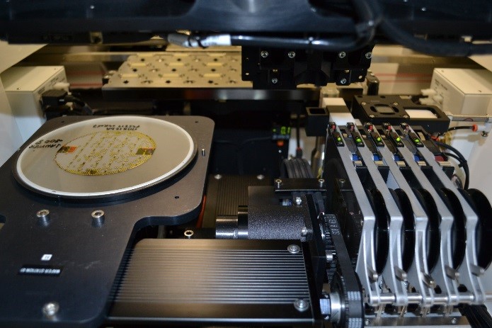
High Accuracy Tape Feeders for Ultra-Small Capacitors
New high precision tape feeders are now available for the presentation of ultra-small capacitors for die bonding. These feeders offer accuracy and performance for handling ultra-small capacitors. The precision feeders are reliable and provide optimum pick efficiency and maximize placement yields for tape fed components. The self-contained feeders include an optical sensor for automatic tape indexing. The indexing sprocket is specially designed and indexed with the resolution needed for ultra-small device tape pockets. Cover tape is carefully removed to avoid any lost parts.
The tape feeders are easy for operators to use, eliminate set up errors, maintain high productivity, and increase capacity. They fit into the standard MRSI die bonding tape feeder bases making field upgrades as simple as inserting the new feeder into an existing MRSI die bonding tape feeder base.
Results
The MRSI Die Bonding family includes the MRSI-705, 5 Micron Die Bonder, and the MRSI-M3, 3 Micron Die Bonder. These die bonding systems offer a complete solution for the successful die bonding of ultra-small capacitors. Key features include epoxy stamping, advanced machine vision, and new high precision tape feeders.
About MRSI Systems
MRSI Systems is a leading manufacturer of fully automated, high-precision, high-speed die bonding and epoxy dispensing systems. We enable customers to optimize the performance of their process including yield, throughput, and uptime by building systems that use our unique expertise. In summary, this includes our proprietary software, proven hardware, deep process knowledge, state-of-the-art manufacturing, and a world-class customer service team. MRSI’s systems are built on common platforms that can be configured to meet specific customer requirements. These platforms are designed to be scalable for R&D prototyping, pilot production and high volume manufacturing. Our solutions deliver the best financial returns in the industry while integrating seamlessly into our customer’s production. Markets include Telecom/Datacom (Data Center), Aerospace & Defense, Medical Devices, Computers and Peripherals, and Industrial. Since 1984, we have been recognized as the standard of the industry, delivering our solutions to leading optoelectronic and microelectronic customers worldwide. We are headquartered in Billerica, MA in the greater Boston area. Our sales are supported by a global network of direct service and support professionals, located in China, Taiwan, Singapore, Korea, Thailand, Malaysia, the Philippines, Israel, Europe, United Kingdom, and the United States.
Subscribe to the MRSI Blog – Weekly Insights into the Advanced Electronic Packaging Industry.