The following excerpt from MRSI Systems latest article published in Laser Focus World Magazine demonstrates how the latest advanced automated die bonding systems are transforming the world of photonics manufacturing –
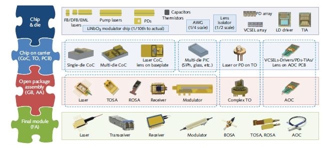
To illustrate our understanding of an automation solution, here is a case study to handle one of the key manufacturing processes — die bonding. Figure 4 is a view of the variety of parts that usually must go through photonics manufacturing. The varieties of these parts result from different types/generations of products to support a wide spectrum of data center communication networks. There are a few major process steps associated with different finished products:

Figure 4 Varieties of parts in photonics manufacturing and examples of groups of automation processes are shown
- For Gold Box products such as transceivers, high-power lasers, typically chip-on-carrier/submount (CoC/CoS) bonding is done first and then the CoC/CoS is bonded onto a common baseplate for lens/mirror attach before putting into a package. The latest trend is that more chips or dies such as the laser, capacitances, and thermistor need to be attached onto a common carrier by either eutectic or epoxy bonding.
- For PCB level of products such as active optical cable (AOC) and onboard optics (OBO), the dies are attached directly onto a PCB. Multiple dies such as a vertical-cavity surface-emitting laser (VCSEL) array, photodiode (PD) array, laser driver, and transimpedance amplifier (TIA) need to be attached on the PCB. The final lens attachment is done by active alignment historically, but now more and more it is done using passive die attach with the availability of high-speed, high-precision (3 µm) die bonding equipment.
- For TO-can-type products, the laser chip and other dies are attached onto a TO base or the vertical post after 90° flipping. To support upcoming 5G wireless deployment, wavelength-division multiplexing (WDM) lasers and electro-absorption modulated lasers (EMLs) are packaged into low-cost TO-can packaging. With many dies that are required to attach, these WDM/EML-TOs are far more complicated than traditional TO-can packaging that only need to handle 1–2 dies.
- For silicon photonics, more processes are transitioning from CoC form to chip-on-interposer and chip-on-wafer (CoW). Much has still yet to be determined, but the future will rest with more and more wafer level integrations.

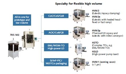
Figure 5 Examples of platform approaches for high-volume and high-mix photonics manufacturing are shown
Figure 5 is an example of how to organize automatic die bonding tools and processes for optimized efficiency. There are three columns in this chart: the left lists all-in-one types of die bonders for R&D and low-to-medium volume; the middle lists the processes consistent with those in Figure 4; and the right lists the specialty types of flexible high-speed die bonders for HVM.
Below are three key points to understand how this approach would help respond to the challenges in photonics manufacturing discussed earlier:
- A common platform at both the hardware and software levels can significantly reduce the NPI risks by eliminating the changes of controls or processes already qualified during the development phase. During R&D/NPI phases, the all-in-one type of die bonding equipment can be used to develop multiple types of products. These automatic machines can handle vast types of dies and processes in one piece of equipment. Their speeds are also fast enough to make low-to-medium levels of volume productions for qualifications of design and manufacturing processes. Once the demand arises and high-volume production is needed, the production lines can be organized into specific process groups.
- High-volume, high-mix photonics manufacturing requires flexible high-volume machines that can cover multiple dies, processes, and products through one machine for one or more process groups. The speed and throughput are optimized by introducing an ultrafast eutectic module and deploying multiple levels of parallel processing, such as separating material handling from die bonding steps and integrating tool changing on the fly with zero time wasted.
- The HVM equipment needs to be built for next-generation products for concurrent fast-pace innovations. In this example, the 3 µm placement accuracy is a step up from current mainstream photonics processes using >5 µm placement accuracy. In addition to enabling new products, high precision in die bonding also increases process yields for manufacturing current products by tightening assembly tolerance as early as possible in the process.
In summary, a high-speed automation platform that does not sacrifice flexibility or accuracy or reliability for 24/7 production is critical to address high-volume, high-mix photonics manufacturing. A common platform between R&D and HVM and the future-proof precision are also critical for fast innovation and reducing NPI risks, and for improving production yields for lower cost in HVM.
The full article can be read here Laser Focus World Article
MRSI Systems continues to bring advanced fully automated die bonding systems to meet the challenges of high tech manufacturers. Following recent product launches in August, MRSI Systems is pleased to announce our “One Stop Shop” die bonding solutions covering the full range of volume and application requirements of manufacturers. Our MRSI-705 (5μm) and MRSI-M3 (3μm) die bonders are historically regarded as the leaders in flexibility. Last year, MRSI Systems introduced the first high speed product – MRSI-HVM3 (3μm) for CoC packaging This year we expanded this product family with the launch of the additional configuration, MRSI-HVM3P for AOC/PCB and Gold-box packaging. In addition, we introduced the MRSI-H3 (3μm) family with specialized configurations MRSI-H3TO for WDM & EML-TO packaging and MRSI-H3LD for high power diode laser packaging. These high speed products deliver the industry-leading speed without sacrificing flexibility, precision or reliability.
Contact MRSI Systems today!

