Die bonding is as old as the semiconductor industry itself. From the onset, integrated circuits or ICs were developed using four levels of interconnections; from bonding of the die, to the end-user product (these four levels are Level 1 – Die Assembly, Level 2 – Printed Circuit Board assembly, Level 3 – Panel Assembly, Level 4 – Final Assembly). Each level of interconnections fans out from a circuit density perspective, from nanometers at the die level, to standard electrical connectors.
Various die bonding approaches have been, and still are, developed to meet the ever-evolving product requirements. Such approaches include:
- Epoxy Die Bonding combined with either batch, continuous or in-situ curing
- Eutectic Die Bonding and in-situ reflow
- Flip Chip Attachment combined with either standalone or in-situ curing
Similar to the die bonding process, the die bonder system varies greatly based on the end product specification requirements. Die bonders for the assembly of high volume consumer products, with its lower reliability and environmental requirements, will consequently be quite different from die bonders dedicated to high reliability telecommunications packages. In the latter case, higher accuracy is required, process repeatability and process control are paramount, and the overall reliability of the interconnect is critical. Therefore, as with all technology purchases, it is essential for prospective buyers of these die bonder systems to be clear on the application requirements.
Market Challenges
Each market has specific challenges for die bonders that need to be considered to ensure optimum performance for the customer. Leading optoelectronic and semiconductor packaging companies require fully automated, high precision die bonders with in-situ capabilities, such as epoxy die attach, eutectic die bonding, and thermo-compression. In addition, given the generational change in volume and bandwidth required from today’s hyper-scale data centers, the market is demanding higher volume and accuracy from these semiconductor packaging companies, more than ever before. Die bonding machines are becoming very sophisticated mini-robotic systems to meet this challenge.
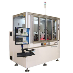
Die bonders are constantly improving with improved speed and accuracy. Our customers are scaling manufacturing capacity to meet increasing business demands, recently driven by data center applications, telecommunication upgrades to 100G+, 5G wireless, and advanced optical sensors. High volume manufacturing of photonic, sensor, and semiconductor devices demands an automatic die bonding system that can deliver industry leading throughput without sacrificing high precision and superior flexibility. Our popular MRSI-HVM high speed, high precision, flexible, 1.5 micron die bonder, has met this challenge with distinction. It is an excellent example of MRSI’s long tradition of combining creativity with solid engineering.
High speed, flexible, 1.5-micron die bonder for high volume manufacturing.
In summary today’s world class die bonder systems need to deliver the following specific outcomes:
- Flexible Component Supply Options – The die bonding system is configured to meet the needs of your supply chain requirements (waffle pack, Gel-Pak®, wafer, tape and reel, and custom trays).
- High Speed AND High Accuracy – An advanced axis system driven by brushless DC linear servomotors with 50nm linear glass-scale encoder feedback for high speeds and accurate movements. The 3-sigma accuracy is better than 1.5 micron.
- High Machine Efficiency AND High Product Quality – Built-in internal temperature monitoring ensures consistent placement.
- Optimum Placement Yields – The system’s closed-loop force control enables placement of delicate devices with as little as 10 grams of force. At the other end of the scale, forces up to 2kg are programmable.
- Maximum Asset Use – Your die bonding system is designed to handle a wide range of processes.
- Strongest ROIs in the industry – A well-established platform with an unmatched Cost of Ownership.
- Extended Machine Lifetime – Exceptional performance over time. Upgrade paths as new features are introduced.
- Proven Manufacturing Readiness – A work horse with minimum downtime. Compelling reliability.
- Configurable Asset – The die bonding system is an open platform that adapts to changing portfolios and can handle complex multi-chip modules and other advanced assembly challenges with ease.
A Die Bonder from MRSI Systems
Die bonding has always been an essential part of the semiconductor supply chain, however as with any early technology products, the curve of innovation demanded of these systems to meet today’s requirements is remarkable. It is therefore essential when considering an investment in a die bonder system that you review all the potential solutions and therefore make an informed investment decision. MRSI Systems will help you make the right choice.