MRSI Systems has been a leading supplier to manufacturers of advanced optical packaging assembly for over 30 years. This has enabled MRSI to build unmatched expertise in the assembly technologies required to successfully produce photonic integrated circuits.
In recent years, the advantage of transferring data with photons instead of electrons, has become a widely accepted methodology for solving the packaging challenges resulting from our growing demand for data and bandwidth. The following post highlights optoelectronics packaging applications.
Optoelectronics Packaging Applications
High Power Laser Diodes (HPLD)
High power laser diodes (HPLDs) cover the broadest range of applications because of many key attributes. HPLDs can offer a wavelength range unmatched by any other laser type ranging from 400nm to 2000nm in optical output range of 1W to 300+W. Furthermore, HPLDs have the highest power conversion efficiency, converting up to 65% of electrical power into laser output power.
HPLD’s require high accuracy products which can handle complex multi-die packages. The MRSI-H3LD fulfills this optoelectronics packaging need with high placement accuracy and internal chip flipping. High precision is essential when placing devices because the optical path must be aligned to minimize the scattering of light. The individual components must be accurately aligned during assembly including aligning the edge-emitting laser to the submount to ensure the beam of light is precise as well as the best possible dissipation of the heat created by chip to a heat-sink submount.
The diodes can be in the form of single emitter or a long bar. The substrate or heat sink submount can be a conventional metal or ceramic block or a special C-mount heat sink. Due to the significant difference in sizes and geometries of diode chips and the heat sink submount, conventional die bonding machine can only handle 1 to 2 types of assemblies. MRSI-H3LD is the only fully automatic die bonder that can handle all three (single emitter on submount, laser bar on submount, and die on C-mount). MRSI-H3LD has <3µm machine placement accuracy and special co-planarity handling for large dies. Both MRSI-H3LD and MRSI-H3LDe can be great candidates for gold-box packaging of high power laser modules – cooled or uncooled.
Active Optical Cables (AOC)
Active Optical Cable (AOC) technology is a cabling methodology that accepts the same electrical input as traditional copper cables, but utilizes optical fiber between the connectors. AOCs use electrical-to-optical conversion on the cable ends to improve speed and distance performance of the cable without sacrificing compatibility with standard electrical interfaces. The basis of AOCs is to embed the active optical transceiver components into the electronic connector instead of using separate optical transceiver and pluggable fiber cable. The manufacturing of AOC components requires high-precision assembly combined with delicate die handling, sophisticated machine vision, automatic material handling, precision epoxy dispensing and in-situ UV curing.
For PCB level of products such as active optical cables (AOC) and onboard optics (OBO), the dies are attached directly onto a PCB. Multiple dies such as a vertical-cavity surface-emitting laser (VCSEL) array, photodiode (PD) array, laser diode driver (LDD), and transimpedance amplifier (TIA) need to be attached on the PCB. The final lens attachment is done by active alignment historically, but now more and more it is done using passive die attach with the availability of high-speed, high-precision (<3µm) die bonding equipment.
The MRSI-M3, 3 micron die bonder is commonly used by OEM and contract manufacturers worldwide for this demanding application. AOC and other PCB Based applications are a specific type of optoelectronics packaging which the MRSI-HVM3P, also a 3 micron die bonder is specifically designed for high speed, high accuracy die bonding for high volume manufacturing. The MRSI-M3, MRSI-H3LD, and MRSI-HVM3P can perform die attaching and lens attaching processes.
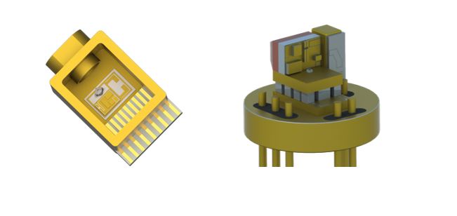
TO-TOSA/ROSA
For TO-can-type products, the laser chip and other dies are attached onto a TO base or the vertical post after 90° flipping. To support upcoming 5G wireless deployment, wavelength-division multiplexing (WDM) lasers and electro-absorption modulated lasers (EMLs) are packaged into low-cost TO-can packaging. With many dies that are required to attach, these WDM/EML-TOs are far more complicated than traditional TO-can packaging that only need to handle 1–2 dies. These new TO-can based devices demand a new class of high speed die bonder that is capable of multi-die and multi-process production in one machine, in order to achieve the best throughput.
The MRSI-H3TO is designed for complex TO assembly including EML/WDM-TO. With the ability to complete multi-die, multi-processing TO-can photonic devices in single path, the MRSI-H3TO product is able to fulfill the needs of effective high volume manufacturing for these complex TO-can products. The new MRSI-H3TO builds on the key technological building blocks featured in our field proven high speed MRSI-HVM3 platform including a dual-head motion system that performs TO pick-and-place/handling and die bonding in parallel. Optoelectronics packaging manufacturers need this high speed die bonder for the next generation of TO-can photonic devices, such as WDM & EML-TOs with industry leading throughput without sacrificing flexibility, accuracy or reliability.
Optical Components and Transceivers
Chip-on-carrier/submount (CoC/CoS) bonding is done first and then the CoC/CoS is bonded onto a common baseplate for lens/mirror attachment before putting it into a package. The latest trend is that more chips or dies such as the laser, capacitances, and thermistor need to be attached onto a common carrier by either eutectic or epoxy die bonding. The MRSI-HVM3 Family is able to handle multi-die, multi-product manufacturing.
For gold-box packaging such as transceivers with high-power lasers, typically chip-on-carrier/submount (CoC/CoS) bonding is done first and then the CoC/CoS is bonded onto a common baseplate for lens/mirror attachment before putting it into a package. More chips or dies need to be attached onto a common carrier by either eutectic die bonding or epoxy die bonding. MRSI-705, MRSI-M1, MRSI-M3, MRSI-H3 Family, and MRSI-HVM3 Family are ideally suited for gold-box packaging.
Silicon Photonics
These devices present unique challenges to meet the increasing market demands. While the challenges are new, volume manufacturing can be achieved using established automation solutions. Common requirements include ultra-high precision placement, in-situ UV curing, advanced vision algorithms, delicate force sensing, material traceability, automated material handling, eutectic bonding, precision dispensing and stamping. Depending upon the methods used, the laser chip can be bonded and coupled to silicon waveguide using <3µm die bonders with passive or active alignments, sometimes flip-chip bonding and self-alignment scheme may be involved. The final lens attachment is done using passive or active die attach with the availability of high-speed, high-precision die bonding equipment. MRSI-HVM3 Family, MRSI-H3LD/MRSI-H3LDe, and MRSI-M1 are great die bonding choices with <3µm machine placement accuracy.
Contact MRSI Systems
MRSI Systems offers a variety of systems for optoelectronics packaging assembly. Leading manufacturers of fully automated, flexible, high-precision die bonding systems require a variety of assembly technologies including epoxy die bonding, eutectic die bonding, thermo-compression, and in-situ UV attach to solve these challenges. An optoelectronics packaging process utilizing proper handling of delicate parts, high precision placement and repeatable assembly platform is necessary. Specifically, MRSI’s die bonders are designed to meet the requirements of optoelectronics packaging applications.
Contact MRSI Systems about your optoelectronics packaging requirements.