This excerpt from MRSI’s recent article emphasizes the CoS die bonding process requirements including geometric placement accuracy and void free eutectic bonding.
Excerpt:
Chip-on-submount
For typical P-side-up CoS die bonding methodology process requirements, the critical CoS dimension, OH, for HPLD die bonding is the laser chip overhang (see Fig. 2) of A (emitter surface line) to C (AuSn surface line). The 10 test CoS build results show the post-bonding accuracy is less than ±3 µm @3σ, with no recess and overhang less than 4 µm.
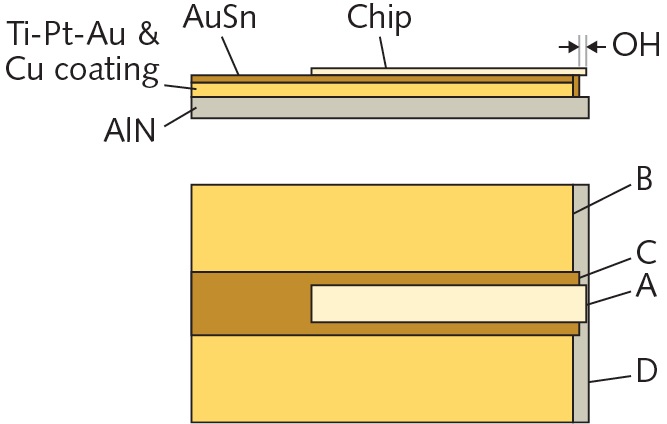
FIGURE 2. For typical P-side-up CoS die bonding, the critical CoS dimension, OH, for HPLD die bonding is the laser chip overhang of A (emitter surface line) to C (AuSn surface line).
In addition to geometrical placement analysis, to detect the percent voids in the solder interface SAM was also carried out on 4 mm × 500 µm × 120 µm laser chip samples of AuSn bonded to an AlN submount. Post-bonding percent voids exceed the MIL-STD 883K Method 2030.2 specification and also pass the more-stringent HPLD percent-voids specification (see Fig. 3).
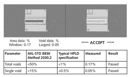
FIGURE 3. The CoS voids test shows that post-bonding percent voids exceed the MIL-STD 883K Method 2030.2 specification and also pass the more-stringent HPLD percent-voids specification.
While placement repeatability, accuracy, and percent voids are vital performance metrics for HPLD die bonding, this capability must be delivered at high speed. A typical temperature profile is used for the eutectic die bonding process; the total cycle time is in the range of 23 seconds or greater than 150 units per hour (UPH).
Read the Laser Focus World article: High-power Laser Diodes: Die-bonder innovations target HPLD manufacturing challenges.