During 2021 CIOE in Shenzhen, China, Infostone, interviewed Dr. Limin Zhou, Senior Strategic Marketing Director of MRSI Systems (Mycronic Group) to discuss MRSI’s latest product developments and some of the key trends in the industry. Below we have captured some of the takeaways from the discussion.
Infostone: Briefly introduce the company and MRSI’s recent development plan?
Dr. Limin Zhou: MRSI Systems (Mycronic Group) is the leading manufacturer of fully automated, high-speed, high-precision and flexible eutectic and epoxy die bonding systems. For over 30 years MRSI has been the standard in the industry for high precision die bonding systems. Over those years MRSI has introduced a number of core technologies, allowing it to provide high-precision, high-speed and highly flexible die bonding solutions ranging from 5 microns to 0.5 microns in accuracy, which can also be configured with different functions to meet customers’ particular application requirements. Our products are used widely in Optical Communication, RF & Microwave ,Aerospace & Defense, Medical Equipment, LiDAR, VR/AR, Optical Transceiver & Silicon Photonics applications. As the market leader with the largest installed base in the industry, deep process engineering experience, and our worldwide local technical support team, we provide the most effective and cost efficient assembly solutions for all packaging levels.
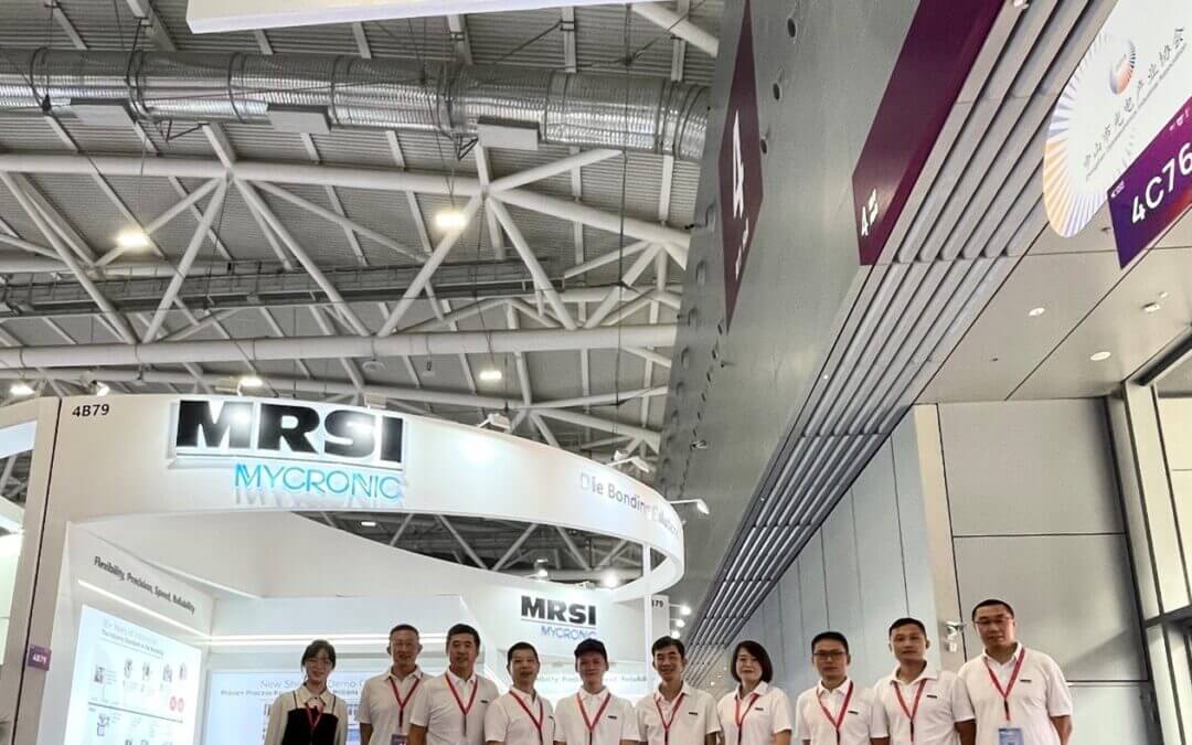
In order to better serve customers in China and Asia, MRSI has set up a new product demonstration center in the Shenzhen Science and Technology Park in Shenzhen, that will be managed locally under a new MRSI legal entity, The center will allow MRSI to carry out localized application development, further enlarge the after-sales service team, and continually improve the spare parts supply chain, in order to respond more quickly to the needs of Chinese and Asian customers.
Infostone: What about the machine demonstration?
Dr.Limin Zhou: This year, we are demonstrating the MRSI-HVM-p die bonder, which has proven to be the best-in-class die bonder with the leading speed, zero-time tool change between dies, and <1.5 micron accuracy, providing the best manufacturing solution for high mix, multi-process optoelectronics production including eutectic, , epoxy die bonding, UV epoxy dispensing and in-situ UV curing. This machine has a fully automatic loading and unloading system, which can support wafer, waffle Pack, Gal Pak® and many other form factors. It has the highest production efficiency in the industry. What I would like to introduce in particular is our patented ”turret with zero time tool change,” which can carry 12 vacuum tips at the same time. The head can be switched automatically in the process of movement, and there is no need for calibration after switching, which greatly saves the process time and improves the production efficiency of multi-chip and multi-process. Our patent protection is global, and the invention patent in China has been effective, which can better protect the intellectual property rights of our invention.
Infostone: What opportunities do you see in the future development, technology and market of the industry?
Dr. Limin Zhou: According to recent Yole and LightCounting reports, the shipment of optical modules increased by 23% in 2020, and it is predicted that the shipments will continue to increase year by year over the next 5-10 years. The optical communication market will face a decade of massive growth opportunities, as new optoelectronic devices emerge one after another, requiring smaller sizes and more integrated packages to achieve lower costs and power consumption. In terms of package form, pluggable devices are still the mainstream of the industry, at least at 800G. However, with the increase of speed and the requirement of low power consumption of devices, pluggable devices will not be able to meet the requirements of low power consumption in the future. Co-Packaged Optics (CPO) will be the packaging development direction of the industry in the future. Regardless of the form of packaging, ultra-high precision passive coupled patches are essential for silicon optical devices. From the perspective of the application of silicon light, it will gradually expand from the application of optical communication to more applications in consumer electronics health monitoring, photon computing and vehicle laser radar. In terms of the trend of silicon optoelectronic device packaging, we find that silicon optoelectronic packaging is also using some advanced semiconductor packaging technology, and the fusion of a variety of packaging technology will be the trend of future development.
Infostone: Please briefly tell us your message and expectation of CIOE China Optical Exhibition.
Dr.Limin Zhou: CIOE China is the largest optoelectronic industry event in China, and also an important platform for MRSI (Mycronic Group) to launch new products. CIOE moved to the Shenzhen International Exhibition Center and the venue’s scale and services have been greatly improved. We thank CIOE for building such a good platform for the optoelectronics industry. We look forward to discussing our common development with the upstream and downstream enterprises in the optoelectronic industry at CIOE.