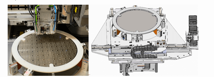
Image: MRSI-S-HVM 300mm wafer table with the wafer frame and an attached 300mm wafer
Advanced heterogeneous integration for 3-D IC packaging, e.g., chiplet, and optoelectronics packaging requires high-precision die bonders that can perform many different processes, such as thermal compression bonding, DAF bonding, BGA/copper pillar bonding, eutectic bonding, hybrid bonding and more. While these techniques are very different from a process point of view, they share many key requirements for bonding equipment, namely:
- Ability to handle up to 300mm Silicon Wafer
- High Placement Accuracy (soon to be below 1µm and may approach 50-100nm for hybrid bonding)
- In-situ Surface Treatment, e.g., plasma treatment, to remove organic contaminants, and oxide, as well as to activate the surface
- Well-controlled heating for a large area from bottom and top, including using a Laser as a Heat Source
- Potentially High Force Bonding with good force and Coplanarity Control
MRSI’s submicron S-HVM die bonder is equipped with a 300mm wafer to handle advanced packaging requirements.
Advanced Packaging Capability Matrix
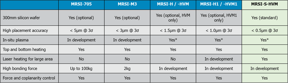
* Die plasma treatment only. Wafer plasma treatment to be developed if it has to be done in-situ. Currently, it is sufficient to treat the wafer offline before bonding.
- Suited for heterogeneous packaging applications.
- Thermal compression bonding · DAF bonding · BGA/copper pillar bonding · Eutectic bonding · Epoxy bonding · Hybrid bonding · Sintering
- Designed for volume production, an easy adaptation from R&D to manufacturing
Sub-micron Ultra High Precision Die Bonder: S-HVM
Key Features
- Auto-switched dual-accuracy-mode placement: <0.5 μm or <1.5 μm
- Mode 1: ±0.5μm @ 3s, with real time alignment (±0.3μm @ 3s achieved)
- Mode 2: ±1.5μm @ 3s, without real time alignment
- 5 μm alignment system liquid-cooled for thermal stability
- Dual head for throughput and flexibility. The left head has a 12-position “on-the-fly” tool changer. The right head has an automatic tool changer with a tool bank.
- Three independent heating sources:
- laser heating
- top heating by bond heat, and
- bottom heating by a bonding stage
- Flip-chip
- Material input: 6” wafer or Gel-Pak®/waffle packs
- Materials output: bond to up to 12 inches (300mm) wafer or custom-designed tray/fixtures
Applications
- Chip-on-wafer silicon photonics bonding, typically with laser soldering
- BGA/copper pillar bonding for 2.5D and 3D packaging
- Hybrid bonding with direct attach
- Optical sensors attach with epoxy
Contact MRSI
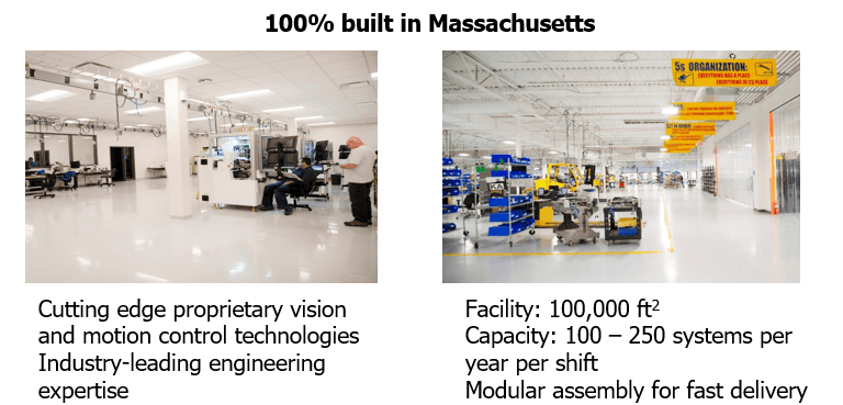
For over 40 years, MRSI has been at the forefront of designing, developing, and manufacturing cutting-edge die-bonding equipment. With a strong track record of delivering high customer satisfaction, we have proudly served customers in aerospace & defense, communications, and medical equipment industries.
Our die bonders are tailored to cater to a wide spectrum of advanced packaging needs for heterogeneous integration. We actively collaborate with industry experts and partners to pioneer innovative packaging processes. To accelerate your journey into the market, we also offer application and prototyping services.
Contact us now to discover more about our die-bonding solutions and to schedule a demo at our headquarters in Tewksbury, Massachusetts.